- David Wessel’s IRCAM
- Organized Entanglement: Fiber and Textile Arts, Science and Engineering
- Managing Complexity with Explicit Mapping of Gestures to Sound Control with OSC
- Notations for Performative Electronics: the case of the CMOS Varactor
- A Synthesizable Hybrid VCO using SkyWater 130nm Standard-Cell Multiplexers
- A Recipe using OSC Messages
- Birds of the East Bay 2020
- Exercising the odot language in Graphics Animation Applications
- C++ container output stream header file
- Programming
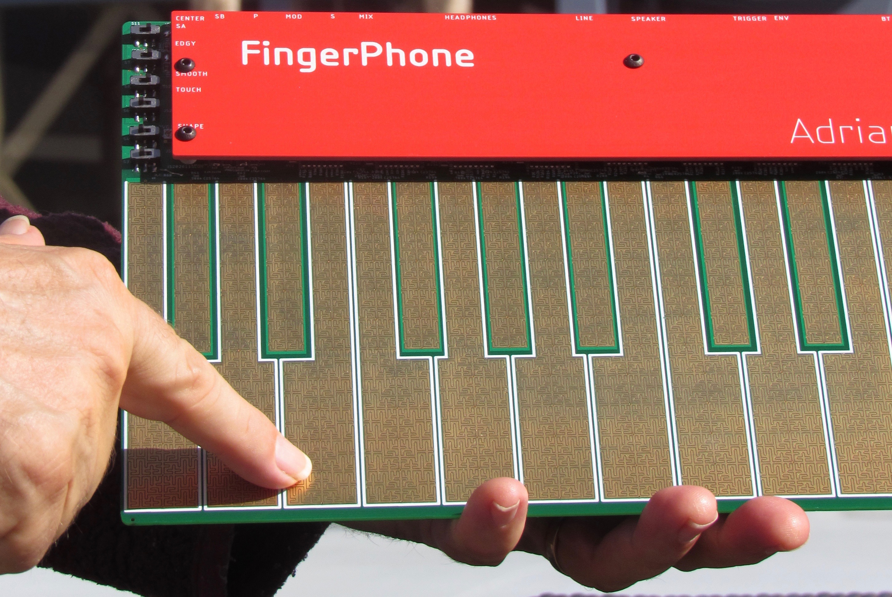
Routing the FingerPhone
Mon, 09/14/2020 - 12:35 — AdrianFreed
Intro
I am studying how IC routing is done in large chips. I am following advice I often give people that it is helpful to learn how to do something by hand before using an automation tool. I was skeptical about this for chip routing because the scale of the problem these routers solve (trillions of gates) is outside what can be done by hand. As it turns out a few of the things I know about routing PCBs helped prepare me for learning some of the conceptual and strategic aspects of what these tools do.These notes make some of these connections using examples of my most recent PCB project, the FingerPhone.
Global Constraints
The FingerPhone board is moderately challenging as boards go. It doesn’t have any high speed (>10Mhz) or very high speed (RF) requirements and it’s not handling high voltages or currents. However it is an audio product so noise considerations are important.
Here are some of the general design constraints:
Partition
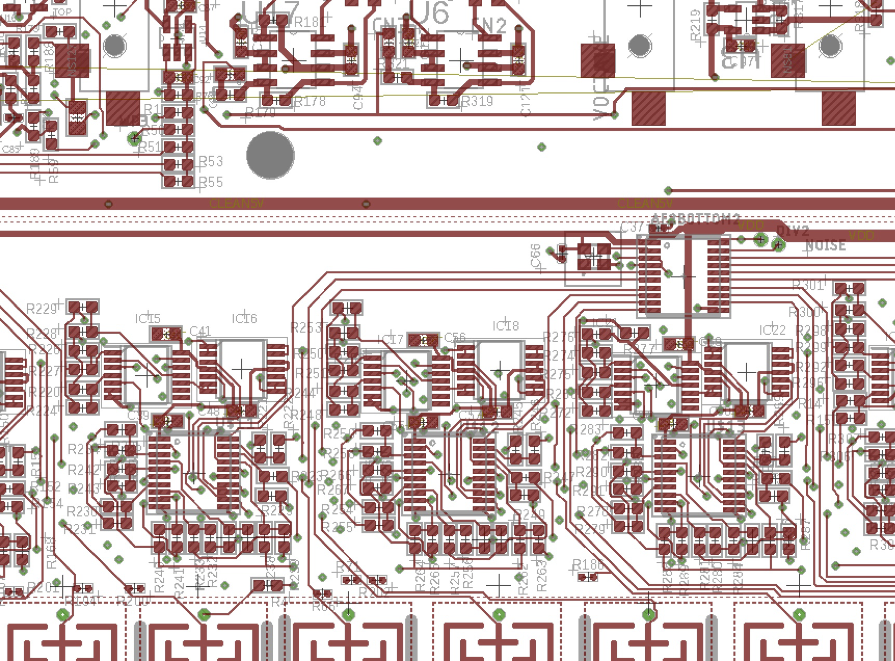
In this project the key partitioning decision was to accept the analog limitations of the mixed signal process available to me for the custom chips and just use that capability for the touch sensor conditioning. One custom chip does top octave synthesis - dividing a master clock into 12 approximately equal tempered square waves. The other (bottom 20-pin device in the picture) does digital synthesis using Walsh functions and the touch sensing. Mixing, panning, frequency, shaping, amplitude modulation are done with non-integrated analog op-amp circuits.Floorplanning and Placement
The partitioning and ergonomic requirements mentioned above help with the floorplanning and component placement. The synthesis chips are close to the keyboard and placed near the three keys they process. The vanilla companion chips which do the amplitude modulation are placed above them and this group of three chips is tiled across the area above the keyboard.This cluster of three chips are spaced apart to make room for a surprisingly large number of resistors which sum the many Walsh function pulse waves into summing buses. There are a lot of them so the outputs can be panned into stereo and so that much of the timbre control can be providing using an organ-stop, additive-synthesis style. I was somewhat comforted by the knowledge that an instrument Bob Moog made using this approach, the PolyMoog, weighs 82 pound.
The summing buses and subsequent analog signals flow to the left, up to the output connectors and then to right to the headphone and speaker amplifiers. Analog processing is completed at the right-most output connectors with an envelope folllower and schmitt trigger for connection to eurorack synthesizers.
Routing
This is the heart of the problem and where most of the time went. Three different styles of routing were required:- The highly geometrically constrained maze patterning of the touch keys
- The regularly tiled routing for the cluster of 3 chips doing the sensing and synthesis The rest around the top edge and sides
Geometrically Constrained Maze
I invented an two-dimensional interdigitation pattern to address a couple of opportunities - only one of which is important in this instrument - to lower the resistance being sensed when you touch the instrument by providing multiple paths for the current to flow. When you look closely you can see a continuous conductor pattern that flows around and floods the “maze". This is the source of the current that will flow through your finger and find the conductors patterned symmetrically around a central spine conductor that flows to the top of each key. Notice there is a via at regular intervals along this “spine”.In other instrument controllers where I use the same pattern, this spine is not continuous - it is a set of vertebra with separate bottom connections made using the vias. In this case mazes for each “vertebra” interdigitate vertically. This affords position sensing and area (pressure) sensing.
The full keyboard involves resolving many different grid related-constraints
The tensions between spacing coprime numbers of things (7 and 12) were an interesting and surprising challenge of the project. I noticed quite a few ugly short cuts in other touch keyboard products and decided to carefully measure how the piano, keyboards and organ in my house expressed solutions - it would be arrogant to ignore 1000 years of keyboard design practice.
The final result is interesting and something I hadn’t really noticed before: the black keys aren’t built to be half way between their surrounding white keys -except for the G# key. Overall you end up with an equivalene class (combining lateral symmetries) with 4 members: (C, F, B, E), (D), (G, A), (all the sharps).
If you have ever taken a piano keybed apart, you may have noticed the keys are stamped with their pitch in case you make the mistake of losing track of where they go. If you find an example when they are not stamped you should mark this on them with a wax crayon or pencil.
The conductor spacing is adjustable in the software via the trace width and flood spacing. With the first instrument I built the spacing was too tight and you could activate chord clusters by simply breathing over the the touch board. Coughing took you into stochastic music territory.
The interdigitation rates are determined by the size of finger you expect to be playing the instrument. The one chosen works quite well for most kids and adults.
The actual layout was done by hand using the grid rounding built into Eagle in the form of tileable modules which are simply pasted by hand into larger assemblies. Each tile is small enought that it is quick to build by hand and the investment in this kit of tiles has been amortized over 4 projects so far.
Routing for the Horizontally-Tiled Center
The tool I am using, Eagle, includes an essential features for this kind of project: the ability to take subcircuits and store them along with their PCB layout. For these 3 chip tiles I was able to experiment with the placement by looking at the results of running the autorouter. Like many affordable CAD programs Eagle has an average-quality autorouter that is fast enough for these sorts of non-committed experiments.There is one strategy I have found serves me rather often dealing with incomplete, congested, weird or ugly routes. What I do is create “white space” around the board until there a set of successful or nearly-complete routes offered. I study these to identify nets which were hard to route and ended up winding around the outside of the placed objects, for example. If these are critical routes I consider hand routing and locking them in before letting the autorouter loose again. Seeing this process dynamically as I reduce surrounding white space can reveal congestion points. These give me hints as to how to change the placement. This may involve adding space around the parts and almost always involves rotating parts. I used to rotate ICs as part of the placement optimization but this often causes questions from the fab. house and increases the chance of erroneously hand installing parts backwards. It’s interesting that in chip placement situations you are constrained about the rotations you can do - standard cells have to sit in tracks, but you can flip them horizontally. Vertical flips result in a track change as the power rails are pre-established. With the FingerPhone most of the rotations were resistors and capacitors.
Because of the tight lead spacing of the ICs there isn’t enough room on the top layer to run all the summing buses. It became clear these would have to run on the bottom and this produced another rather common approach in chip routing called Manhattan routing where each routing layer has a preffered direction. This requires vias from the top to the bottom for every summing resistor so it was necessary to create enough white space for these vias. Much of the top routing is vertical.
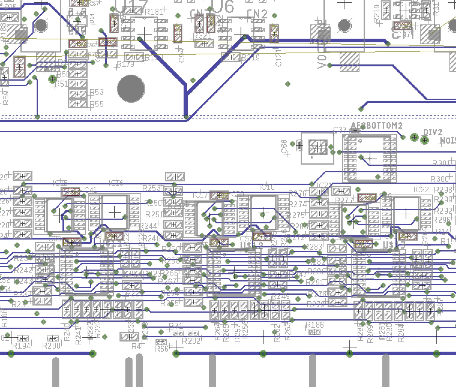 A nice feature of having untented vias in the prototypes
is that these buses were available for probing and by cutting traces on the bottom circuits could be isolated for debugging.
A nice feature of having untented vias in the prototypes
is that these buses were available for probing and by cutting traces on the bottom circuits could be isolated for debugging.
I would like to think this helps me think about DFT (Design For Test) strategies in chips.
It’s worth mentioning that I had some control over the pin assignment of the custom chips and some tuning of this was informed by the placement and routing. This helped me appreciate that some standard cell libraries provide for more via attachment points on their nets than others. It’s interesting because it suggests a high-density standard cell library is more difficult to route because it provides for more functionality in a smaller area to route and also has to contend with less flexibility as to where the vias attach.
Routing the Rest
If it wasn’t for analog circuit layout practice the rest of the board could have been autorouted. It’s hard to teach medium-quality autorouters about guard rings, decoupling, ground plane management and other strategies to minimize noise and crosstalk. Again I used the autorouter to give placement optimization hints but resorted to hand routing for the details.Normally you would like to protect the input of opamps from stray signals. One of the main uncertainties of this design is that this isn’t easy when the summing busses go 2/3rds the length of the board. To mitigate the problem and the need to rev. the board to use fancier grounding (e.g. going to 4 layers), I lowered the impedance at the expense of higher current. This is a two-edged sword because the higher currents may induce more noise. The final results were satisfyingly quiet - better than traditional organ designs - presumably because the board is smaller and voltage levels are so much lower and closer to the output voltage levels. Old organs often ran with 10-30volt rails. Here I am using 3.3V and +- 3.3V
Conclusion
As I delve into the literature on IC routing, I see that what I have been improvising is similar to what a global router does. At the least it will inform iterations necessary with placement and at best it also provides a viable seed route for the detail router. In the PCB case - unless the board is small or has uncritical performance requirements, I am the detail router. I riff on the approximate routing from the autorouter.I remain skeptical of my own process. I was very influenced as a young computer scientist by a famous paper on a small classical resource assignment problem. They asked the experts on this problem around the world to submit their solution. None of them were better than random assignment. I develop theories and heuristics on how to proceed on a given project but I have to remind myself they could be good be poor and a long way from optimal and also may not apply on the next project.
However I was encouraged to learn that some of these heuristics have been already discovered and explored in professional routing tools. For example, ripping up and rerouting is often necessary but when I do this by hand I try to use the knowledge from previous routes. Many routers dont do this because of the cost of storing and using the prior information. Some routers are structured to be able to do this and the history does indeed help.
The limitations of individual knowledge of routing problems are obvious - you don’t have enough personal designs to say anything useful about how well algorithms work. Key progress in this area has come from pooling large numbers of representative designs and benchmarking routers with them in annual competitions.
One of the things I enjoy about Jin Hu's 2013 dissertation is the careful account of how these benchmarks can be done avoiding the classical gaming of recognizing the benchmark design and tweaking parameters. Their global router performers comparatively well without expert tuning. They offer comparisons where they defeat the custom tuning of competitive routers in competition datasets.
"High-performance Global Routing for Trillion-gate Systems-on-Chips", Jin Hu, 2013, University of Michigan
| Attachment | Size |
|---|---|
| pcbTop.png | 2.45 MB |
| pcbBottom.png | 1.68 MB |
- AdrianFreed's blog
- Login or register to post comments
- Printer-friendly version